
In today’s high-performance electronic devices, reducing electrical noise is essential for ensuring the reliability and efficiency of circuit boards. Electrical noise, or electromagnetic interference (EMI), can degrade the performance of a system, affecting signal integrity and overall functionality. Gold finger PCBs (Printed Circuit Boards) have become increasingly important in combating electrical noise, especially in applications where high-speed data transmission and low signal loss are critical. This article will explore how Gold Finger PCBs reduce electrical noise, providing users and consumers a clearer understanding of their benefits in electronic designs.
Understanding Gold Finger PCBs and Their Role in Electronics
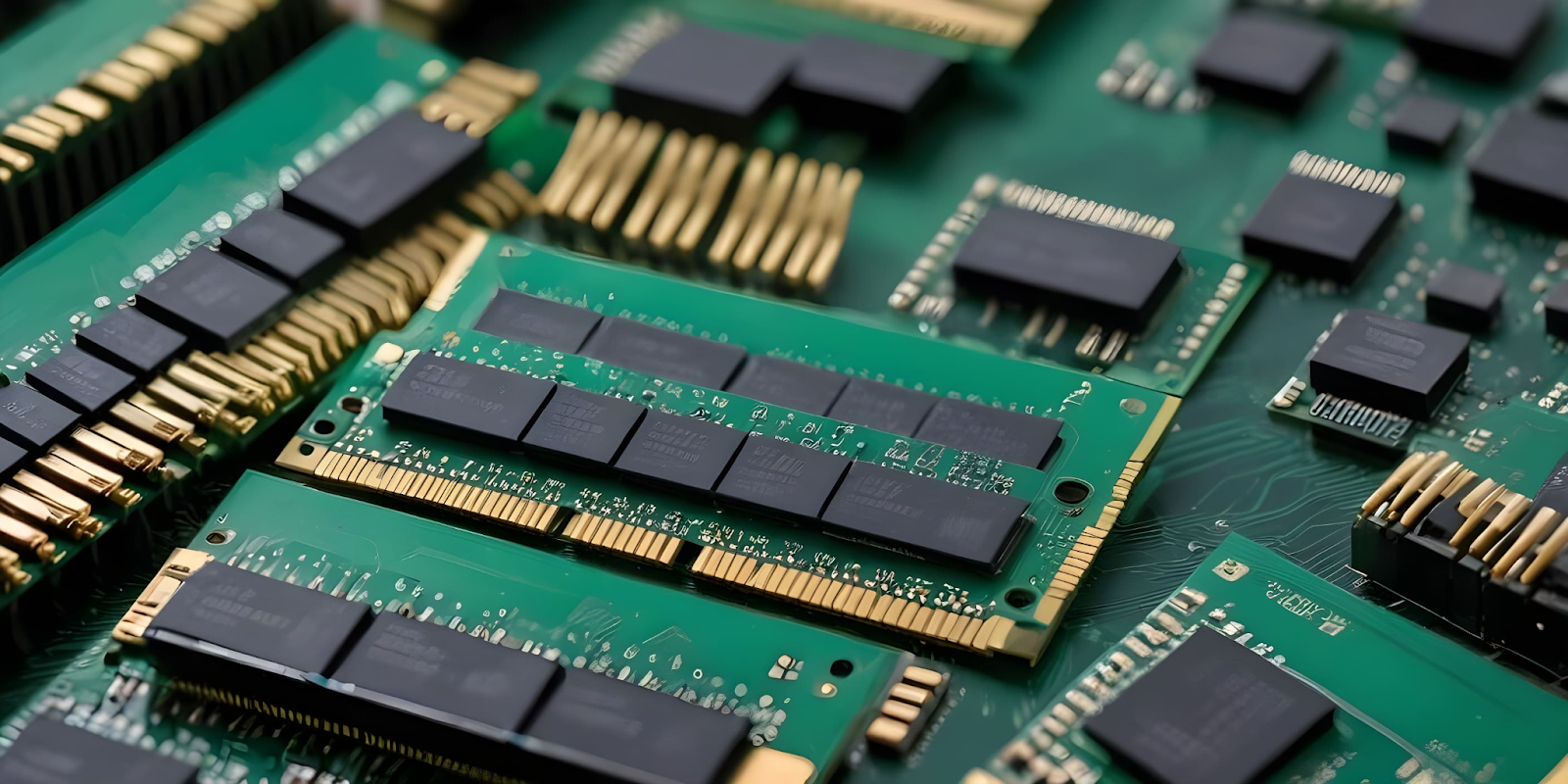
A Gold Finger PCB is a specific type of PCB that incorporates gold-plated connectors or “fingers” at its edges. These gold fingers are primarily used for reliable, high-performance connections in devices such as memory modules, graphics cards, and other high-speed electronics. Gold is chosen for its excellent conductivity, corrosion resistance, and durability, which are crucial for ensuring a strong electrical connection.
In Gold Finger PCBs, the gold plating is applied to the exposed edges of the PCB, where connections are made to external components. The gold plating ensures that the connectors remain free from corrosion, which can cause poor electrical contact and potential signal degradation. Beyond providing reliable connections, gold fingers also help to mitigate one of the most significant challenges in high-speed circuit design: electrical noise.
Electrical noise can significantly affect performance when designing PCBs, especially those in high-frequency applications. This can lead to signal degradation, data corruption, or even system failure. Gold Finger PCBs address this issue by offering superior conductivity and minimizing contact resistance, which can help prevent the generation of unwanted electromagnetic interference (EMI).
How to Improve Signal Integrity
Signal integrity is critical in high-speed digital applications like communications and computing devices. Any disruption or degradation of the signal can cause performance issues, such as latency, data loss, or errors in processing. Gold Finger PCBs play a crucial role in enhancing signal integrity by providing stable, low-resistance connections between components, which reduces the likelihood of signal loss or distortion.
The gold plating on Gold Finger PCBs helps maintain consistent electrical contact, even at high frequencies. As a result, the PCB minimizes signal reflection and voltage drop, which are common issues in high-speed circuits that can lead to noise. A well-designed Gold Finger PCB provides clean signal paths, ensuring efficient signal transmission without external or internal noise interference.
Moreover, gold plating’s excellent resistance to oxidation and corrosion also helps maintain signal integrity over time. In PCBs that lack proper protective coatings, connectors can degrade, leading to poor connections that introduce noise into the system. Gold Finger PCBs avoid this issue because the gold plating keeps the connectors intact, allowing them to handle high-frequency signals with minimal interference.
Reduce EMI and Crosstalk
Electromagnetic interference (EMI) and crosstalk are common sources of electrical noise that can degrade circuit boards’ performance. EMI refers to unwanted electromagnetic signals that disrupt the normal functioning of electronic components, while crosstalk is the unwanted transfer of signals between adjacent traces or wires. Gold Finger PCBs help reduce these types of noise in several ways.
First, the gold fingers act as effective shields, preventing the spread of EMI across the board. Their high conductivity and low resistance properties help contain electrical signals, ensuring they don’t leak and interfere with neighbouring circuits. This is particularly important in devices like memory modules or high-speed processors, where the slightest interference can lead to data corruption or processing errors.
Furthermore, Gold Finger PCBs can be designed with appropriate ground planes and signal routing to reduce the potential for crosstalk. By carefully controlling the placement of components and optimizing the routing of signal traces, designers can prevent signals from coupling into adjacent circuits, which would otherwise result in noise. The well-designed signal paths and high-quality gold connectors ensure that Gold Finger PCBs maintain excellent performance in environments with high EMI levels.
Improves power delivery and reduces noise
Power delivery is another critical area where Gold Finger PCBs reduce electrical noise. In high-performance systems, stable power is essential to prevent fluctuations that could introduce noise into the signal lines. Gold Finger PCBs help optimize power delivery by providing low-resistance, stable connections between power sources and critical components.
The gold-plated fingers reduce the chances of voltage drop or power surges that can cause noise, ensuring that the power supply remains steady and clean. When power delivery is stable, the likelihood of noise generation decreases significantly, improving the system’s overall performance. This is especially important in applications that require precise and reliable power, such as medical devices, communication equipment, and data centres.
By using Gold Finger PCBs in power-critical applications, manufacturers ensure consistent power delivery without introducing unwanted fluctuations that could interfere with sensitive components’ operation. This leads to a more stable and noise-free system, increasing the device’s longevity and reliability.
Durability and lifespan in terms of noise reduction
The durability of Gold Finger PCBs is another key factor in their ability to reduce electrical noise. Gold’s natural resistance to corrosion and oxidation ensures that the connectors maintain their integrity over long periods of use. In contrast, other materials may degrade over time, leading to increased resistance at connection points and the potential introduction of noise.
As electronic devices continue to be used in more demanding environments—such as automotive systems, industrial machinery, and high-performance computing—the ability to withstand harsh conditions without compromising performance becomes even more critical. Gold Finger PCBs are designed to handle the rigours of these environments, maintaining their conductivity and reducing the risk of noise due to corrosion or wear.
The longevity of Gold Finger PCBs contributes to consistent signal integrity and reduces maintenance costs. Devices built with Gold Finger PCB is less likely to experience performance issues due to connector degradation, leading to fewer system failures and longer device lifespans. This durability ensures the device continues to function optimally, even in environments with high electrical noise.
Applications in high-speed and sensitive devices
Gold Finger PCBs are essential in various applications where electrical noise can significantly impact performance. For example, in memory modules, where high-speed data transfer is critical, the gold fingers provide stable, low-resistance connections that ensure the memory operates optimally. Any electrical noise or signal degradation could result in slow performance or data corruption, making the need for clean, reliable connections vital.
In high-speed communication devices such as graphics cards, networking equipment, and storage devices, Gold Finger PCBs help maintain the integrity of fast signals and prevent interference that could affect data transmission. Reducing electrical noise is paramount to maintaining performance in these applications, as even small amounts of noise can cause significant issues in high-speed systems.
Gold Finger PCBs are also beneficial in sensitive industrial equipment, where electrical noise can lead to malfunctioning or inaccurate readings. For instance, in medical devices, reducing electrical noise is critical for ensuring the accuracy of diagnostic tools and patient monitoring systems. Gold Finger PCBs enable these devices to perform reliably by reducing interference that could lead to false results.
The Critical Role of Gold Finger PCBs in Reducing Electrical Noise
In conclusion, Gold Finger PCBs are vital in reducing electrical noise and ensuring the efficient operation of high-performance electronic devices. These PCBs’ high conductivity, low resistance, and excellent durability help reduce EMI and crosstalk, ensuring that signal integrity remains intact even in challenging environments. They also play a crucial role in optimizing power delivery, preventing voltage fluctuations that could introduce noise.